ADC和DAC那些事儿
1 Offset and Gain Error
1.1 BOOK 1
ANALOG INTEGRATED CIRCUIT DESIGN(Tony Chan Carusone, David A. Johns, Kenneth W. Martin)
1.2 ARTICLE 1
ADC Offset and ADC Gain Error Specifications July 17, 2022 by Dr. Steve Arar
When assessing certain non-ideal effects, such as offset error, gain error, and nonlinearity, it is useful to model the ADC transfer function by the straight line that goes through the midpoint of the steps.
ADC Offset Error and the Transfer Function
Due to non-ideal effects like a mismatch between internal components, the actual transfer function of an ADC deviates from the ideal staircase response. The offset error shifts the transfer function along the horizontal axis and hence causes a shift in the code transition points.
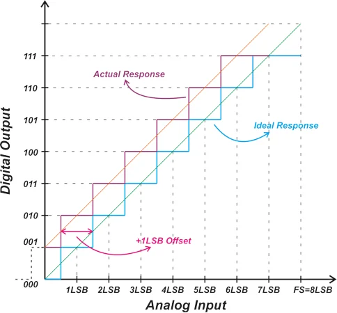
For a unipolar three-bit ideal ADC, the first transition should occur at 0.5 LSB, changing the output from 000 to 001. However, with the above response, the ADC output transitions from 001 to 010 at 0.5 LSB. The 001 to 010 transition should ideally occur at 1.5 LSB. Therefore, the non-ideal response is shifted by 1 LSB to the left when compared to the ideal characteristic. This is described as +1 LSB offset error. Considering the linear model of the non-ideal response (the orange curve in the figure), we can also observe that the system outputs 001 for a 0V input, corresponding to +1 LSB offset.
Since the offset error shifts the entire transfer function by the same value, it can easily be calibrated out by subtracting the offset value from the ADC output. To determine the offset error, the first code transition is usually measured and compared with its corresponding transition from the ideal response. Using the first code transition (rather than the next ones) results in a more accurate measurement because the offset error by definition refers to the deviation from the ideal response at zero volts input.
ADC Gain Error
With the offset error eliminated, the first transition of the actual response coincides with that of the ideal characteristic. However, this doesn’t guarantee that the other transitions for the two characteristic curves will also occur at the same input values. The gain error specifies the deviation of the last transition from the ideal value.
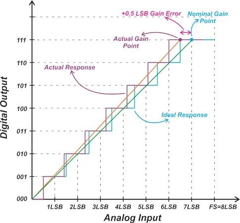
Let’s define half LSB above the last transition as the “gain point.” With the offset error eliminated, the difference between the ideal gain point and the actual gain point determines the gain error.
In the above example, the non-ideal characteristic has a gain error of +0.5 LSB. The orange curve in the above figure is the linear model of the non-ideal response. As you can see, a difference between the measured gain point and the ideal gain point actually changes the slope of the linear model of the system.
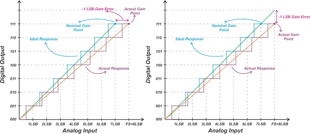
Note that ADC Gain Error define the gain error as the vertical difference between the actual gain point and the straight line model of the ideal ADC. Both the vertical and horizontal differences yield the same result because the ideal linear model has a slope of one.
Expressing Gain Error in Terms of Full-Scale Error
Building on the concepts discussed above, we can define the gain error in terms of the full-scale error. This is illustrated in Figure 7 from Microchip.
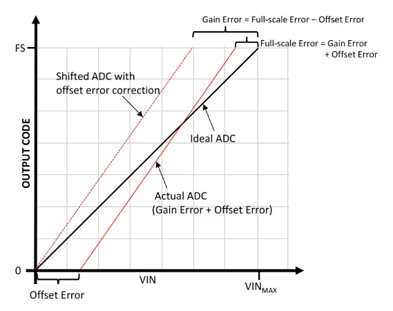
In the above figure, the actual response is affected by both offset and gain errors. Therefore, the deviation of the actual last transition from the ideal last transition, which is denoted by full-scale error, contains both offset and gain errors. To find the gain error, we can subtract the offset error from the full-scale error:
This is equivalent to first compensating for the offset error and then measuring the deviation of the last transition from the ideal response to arrive at the gain error. Note that in this particular example, the gain error is positive and the offset error is negative, leading to a full-scale error smaller than the gain error.
Some ADC Specification Inconsistencies in Definition
It is worth mentioning that some ADC specifications are not consistently defined in technical literature. One confusing inconsistency is the sign of the offset and gain error. For example, while Microchip and Maxim Integrated are consistent with the definitions used in this article, some manufacturers, such as STMicroelectronics (ST), differ. ST defines the sign of these error terms in the opposite way. Inconsistencies are also observed between documents from the same chip manufacturers. For example, Figure 8 is taken from this Texas Instruments (TI) document that uses the opposite sign convention.
The sign convention used in Figure 9 (and throughout this article) seems to be more widely accepted in various technical literature. Despite this. such inconsistencies can cause confusion, though you can get around the problem if you’ve grasped the basic concepts discussed in this article. For example, if you measure an ADC and observe that its first transition occurs above 0.5 LSB (similar to the case depicted in Figure 3), you know that an appropriate positive value should be added to the ADC reading to compensate for the offset error, regardless of the sign convention you are using.
1.3 MANUFACTURER 1
1.3.1 ARTICLE 1
Understanding Data Converters, Application Report, 1995
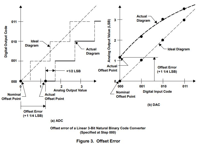
3.1 Offset Error
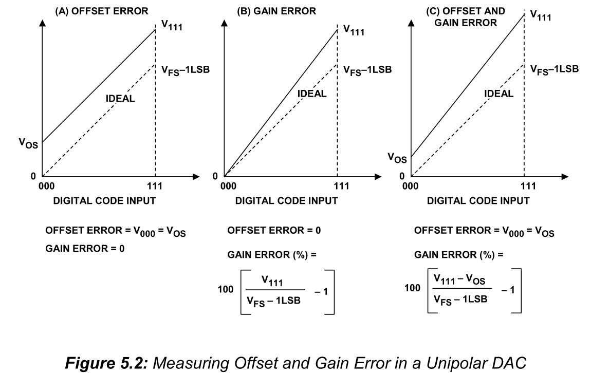
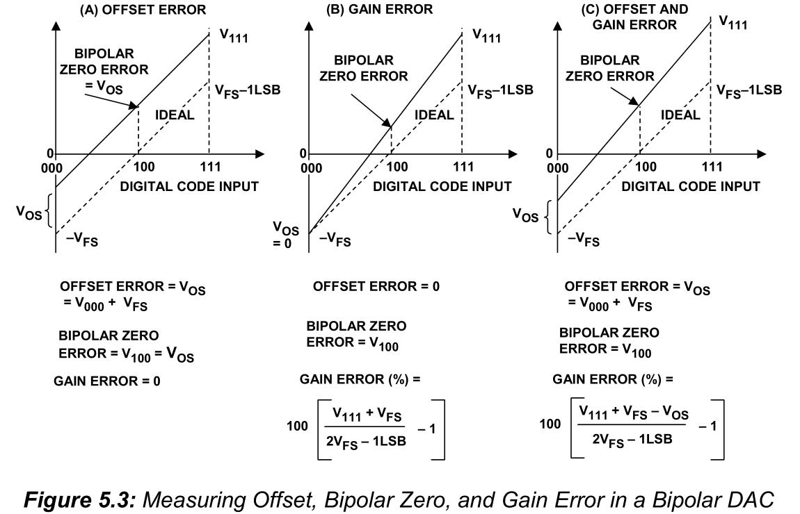
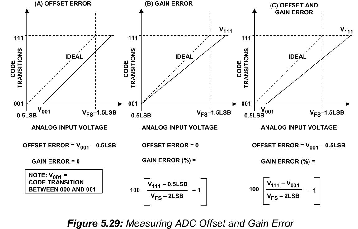
The offset error as shown in Figure 3 is defined as the difference between the nominal and actual offset points. For an ADC, the offset point is the midstep value when the digital output is zero, and for a DAC it is the step value when the digital input is zero. This error affects all codes by the same amount and can usually be compensated for by a trimming process. If trimming is not possible, this error is referred to as the zero-scale error.
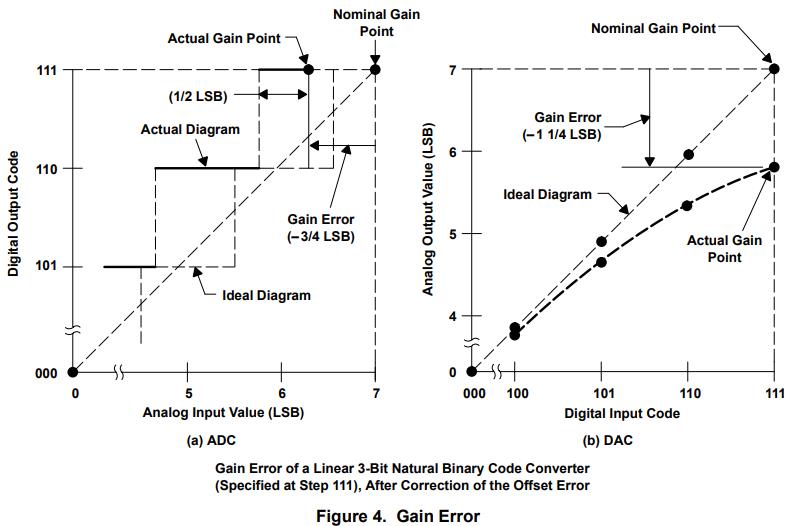
3.2 Gain Error
The gain error shown in Figure 4 is defined as the difference between the nominal and actual gain points on the transfer function after the offset error has been corrected to zero. For an ADC, the gain point is the midstep value when the digital output is full scale, and for a DAC it is the step value when the digital input is full scale. This error represents a difference in the slope of the actual and ideal transfer functions and as such corresponds to the same percentage error in each step. This error can also usually be adjusted to zero by trimming.
1.3.2 ARTICLE 2
TI Precision Labs > TI Precision Labs - Data converters > Analog-to-digital converters (ADCs) > Introduction to analog-to-digital converters (ADCs) > AC & DC specifications: Offset error, gain error, CMRR, PSRR, SNR and THD
2.2 AC & DC specifications: Offset error, gain error, CMRR, PSRR, SNR and THD
adcs-ac-and-dc-specifications-offset-error-gain-error-cmrr-psrr-snr-thd-presentation-quiz.pdf
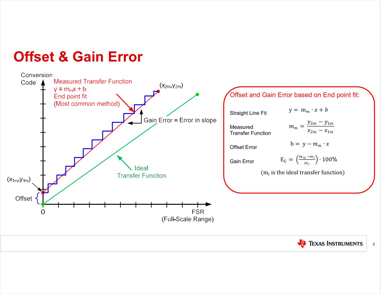
Let’s start with the basic calculation for offset and gain error. The key to understanding this is to know that the ADC transfer function is not perfectly linear. So a linear fit curve is applied to the function. For this calculation, the most commonly used type of curve fit is an endpoint linear fit. With this type of curve fit, the first and last points on the ADC transfer function define the straight line.
Recall that a straight line has the equation y equals mx plus b. Also the slope can be calculated by taking the change in y divided by the change in x. Sometimes this is referred to as the rise over run.
The offset is the Y-axis intercept. That is, the offset is the value of the transfer function when x equals 0. This value can be calculated by rearranging the equation y equals mx plus b and solving for b where b is the offset.
The gain error is the percentage difference between the ideal slope and the measured slope. The gain error and offset error are often referred to as DC errors, as they can be measured with DC input signals plot.
1.3.3 ARTICLE 3
TI Precision Labs > TI Precision Labs - Data converters > Analog-to-digital converters (ADCs) > Error sources > Understanding and calibrating the offset and gain for ADC systems
5.2 Understanding and calibrating the offset and gain for ADC systems
adcs-understanding-and-calibrating-the-offset-and-gain-for-adc-systems-presentation-quiz.pdf

1.3.4 ARTICLE 4
TI Precision Labs > TI Precision Labs - Data converters > Digital-to-analog converters (DACs) > DACs in application > Precision DAC calibration
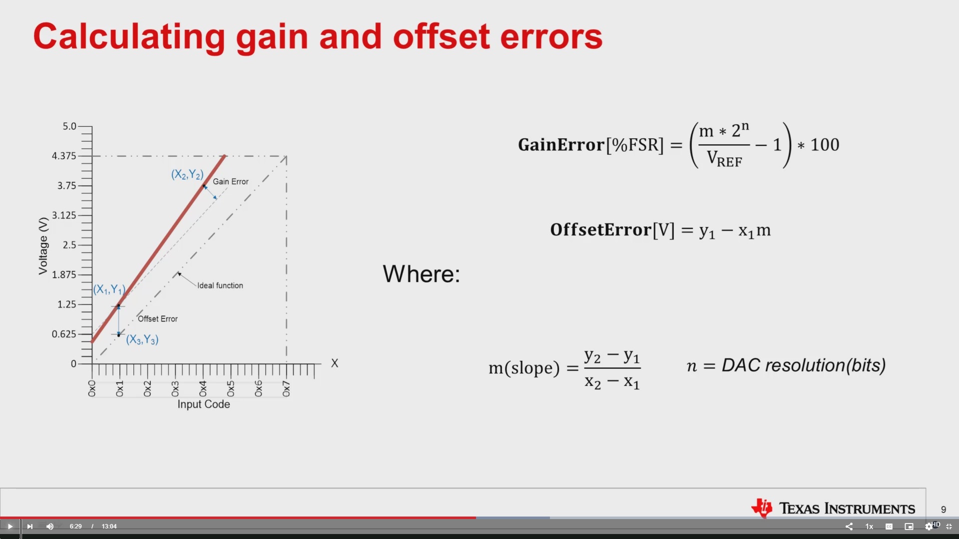
Calibration is done in the linear region of the DAC because this is where the offset and gain errors are actually measured. DAC gain error and offset error are calculated as follows. As each DAC datasheet specifies the actual codes at which each measurement is taken, this makes it very easy to calculate the actual gain and offset errors based on the noted equations where slope m is the slope of the actual output function, and n equals the resolution of the specific DAC. Again, gain error is measured in percent Full Scale Range, or FSR, while offset error is measured in volt units. Next, we will discuss actual calibration of DAC.
1.4 MANUFACTURER 2
1.4.1 ARTICLE 1
《The Data Conversion Handbook》, 2005
Chapter 5: Testing Data Converters
1.4.2 ARTICLE 2
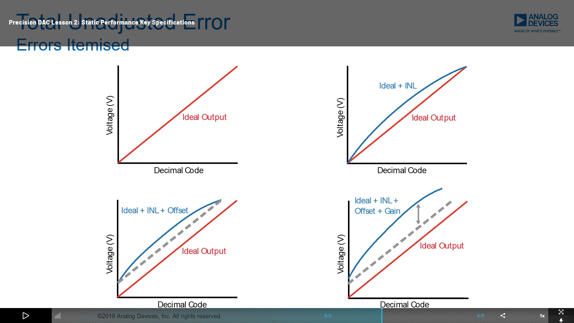
Precision DAC Lesson 2: Static Performance Key Specifications